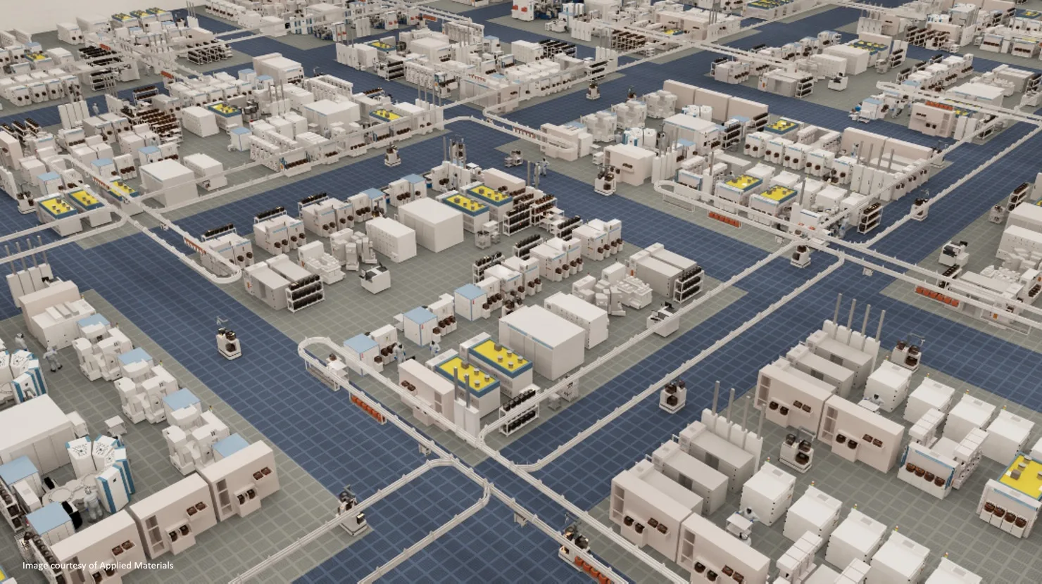
Applied Materials and NVIDIA have collaborated to develop an end-to-end digital development model for semiconductor innovation. This model unifies atomic-scale discovery, process engineering, and factory optimization by integrating GPU-accelerated platforms such as Ginestra with cuDSS, cuEST, PhysicsNeMo, and Omniverse. The collaboration leverages NVIDIA CUDA-X libraries to accelerate various aspects of semiconductor design and manufacturing.
Key Points
- Applied Materials and NVIDIA integrated GPU-accelerated platforms to create an end-to-end digital development model.
- The model unifies atomic-scale discovery, process engineering, and factory optimization.
- NVIDIA CUDA-X libraries accelerate materials simulation, density functional theory workflows, multiphysics process modeling, and digital twin creation.
- Quantum chemistry simulations show up to 55x speedups.
- Chamber simulation times have improved by up to 35x.
- Ginestra, a physics-based simulation platform, connects material properties and defects to predicted device performance.
- Integrating NVIDIA cuDSS into Ginestra accelerates sparse linear algebra, delivering up to a 10x speedup over CPU-only approaches.
- NVIDIA cuEST accelerates demanding steps of the density functional theory (DFT) workflow.
- Simulations that took five days on 64 CPU cores can now be completed in approximately two hours on a single GPU using NVIDIA B200 systems.
Context
According to the NVIDIA Developer Blog, increasing AI workloads are driving explosive compute demand, pushing the semiconductor industry to meet unprecedented performance targets. The shift from chip-level optimization to system-level engineering is compounding thermal and power challenges. Meeting these demands requires breakthroughs in materials deep within the device stack, necessitating advanced modeling and simulation beyond conventional approaches.
Why It Matters
This collaboration enables semiconductor engineers to rapidly explore material-property-performance relationships, optimize process recipes, and validate fab-wide operational strategies virtually. This approach drives faster iteration cycles and reduces reliance on costly physical experiments, addressing the need for rapid innovation in semiconductor manufacturing.
What To Do
- Note the specific NVIDIA CUDA-X libraries mentioned (cuDSS, cuEST, PhysicsNeMo) for accelerating materials science workflows.
- Compare the stated speedups (e.g., 55x for quantum chemistry, 35x for chamber simulation) against current CPU-based simulation times.
- Investigate how the integration of NVIDIA cuDSS into platforms like Ginestra can accelerate sparse linear algebra in simulations.
- Watch for further developments in the use of NVIDIA B200 systems for accelerating complex scientific computations.
Keep Exploring
/atlas/image-models